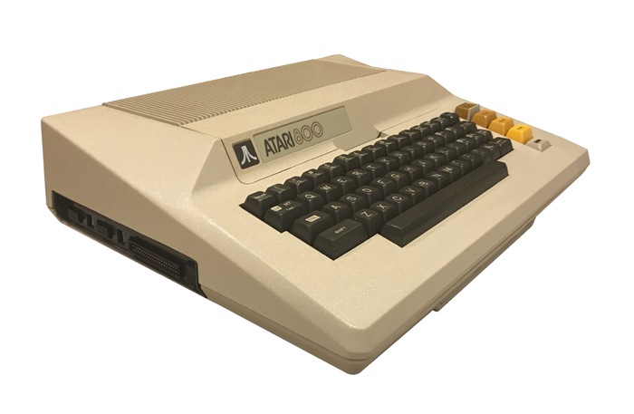
| The Atari 800D appears to be
a modified Atari 800 computer system with a different CPU
Board that passes through the Bus signals over to a board
that occupies the previously unused Left section of the
Atari 800 case. The
left side of the Atari 800 case is redesigned to accommodate
this new Left Side panel. A Ribbon cable from
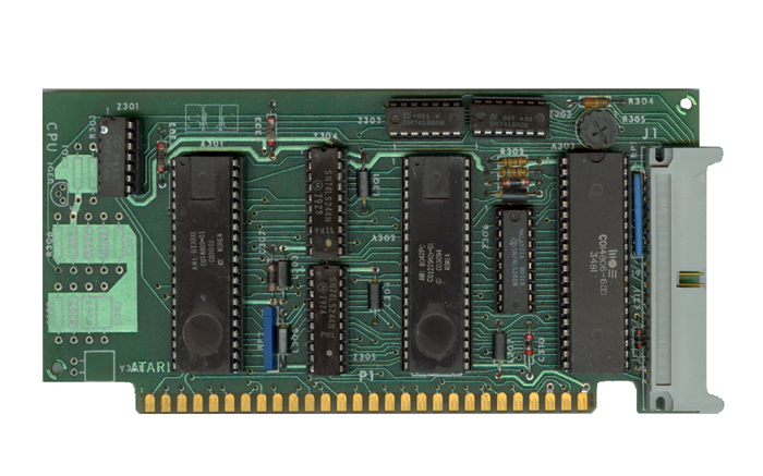
the CPU feeds over to the Left Side Interface board.
The System BUS signals pass through the Left Side Interface
board and go out through a 40 pin connector. This
appears to be the first implementation of the Atari "PBI"
(Parallel Bus Interface) on any Atari computer system.
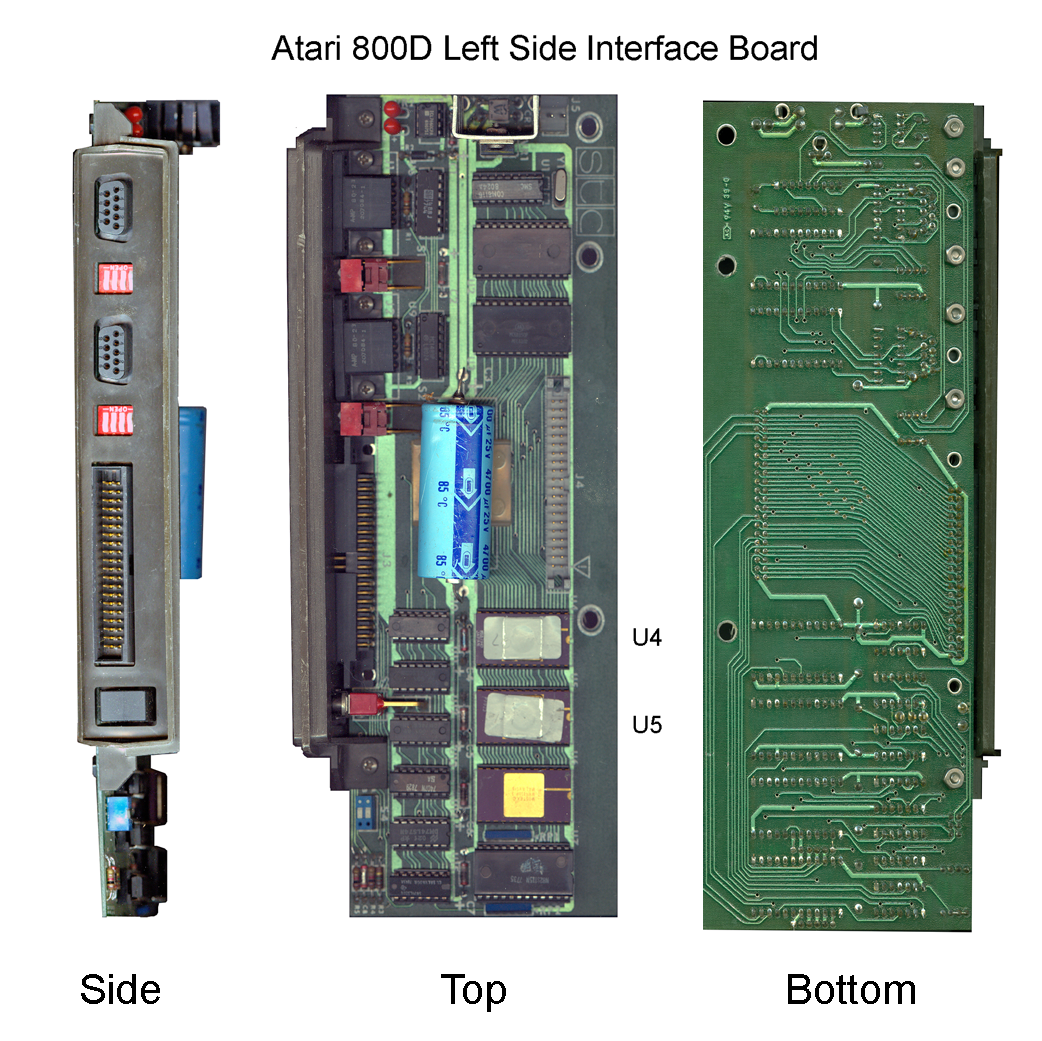
On the Left Side Interface
Board there are also 2 DB9 connectors which are tied in with
a pair of MC6850 Asynchronous communication adapter (ACIA)
chips. There is also an SMC 8116 Baud Rate Generator.
2 ROM chips located at IC
locations U4 and U5 supply the device drivers for the board.
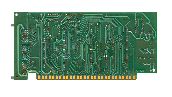
Essentially what Atari did
was provide the Atari 800 with built in Serial communication
ports and an External Expansion port. |